Equipment:
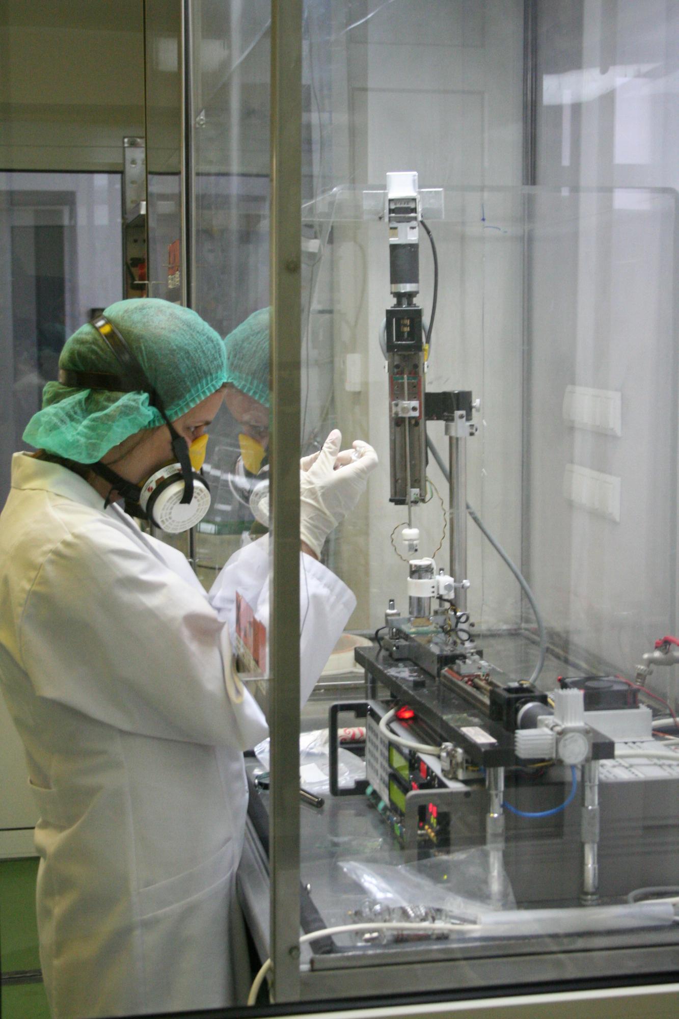
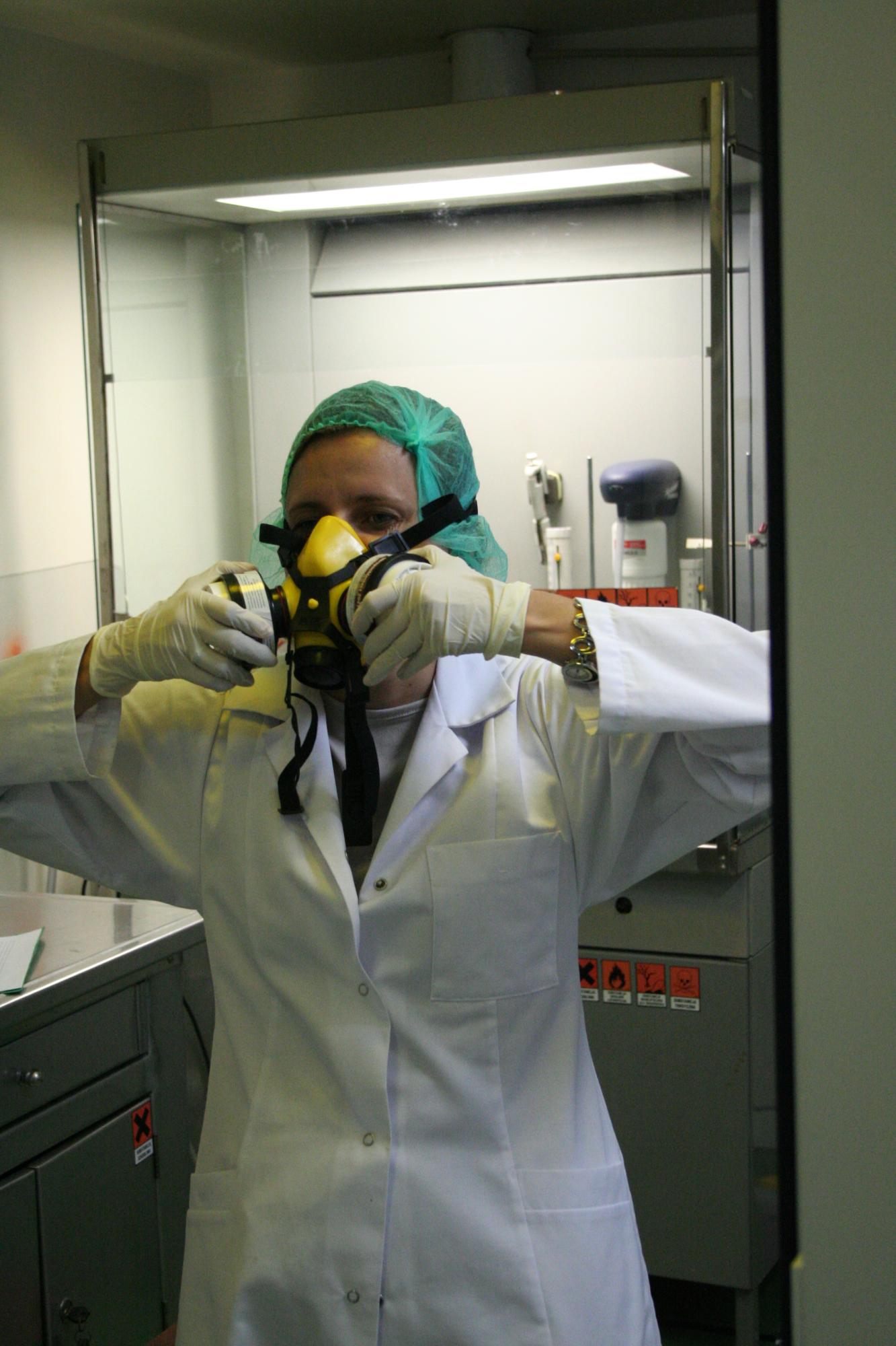
- Clean-room facility with equipment
Parameters - equipment includes:
- System for thin layers fabrication Zone Casting technique
- System for thin layers fabrication Spin Coating technique
- Low pressure plasma cleaner (Atto, Diener Electronic)
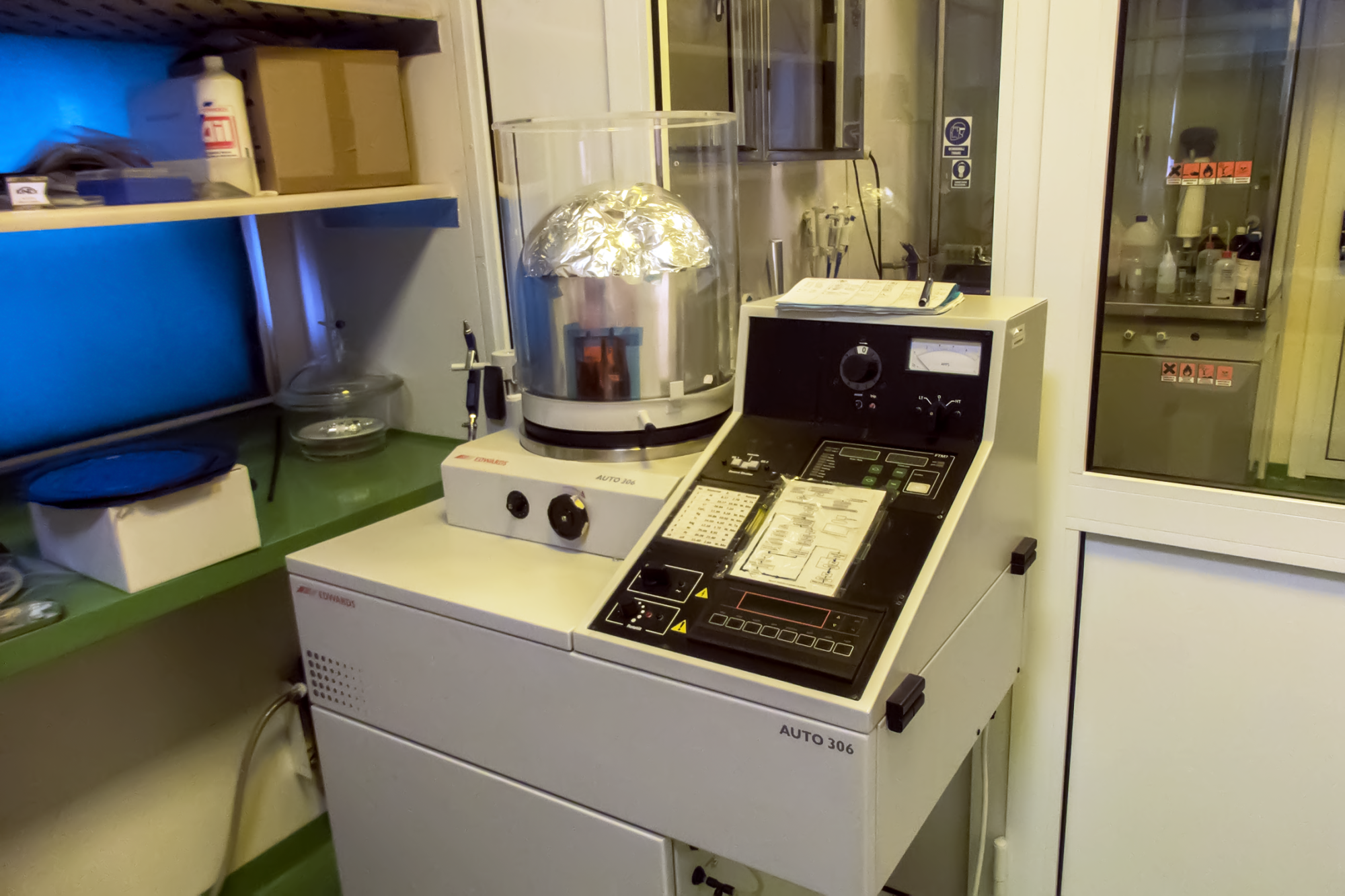
- Vacuum evaporation system Edwards Auto 306 Turbo
- System for field-effect transistors measurements
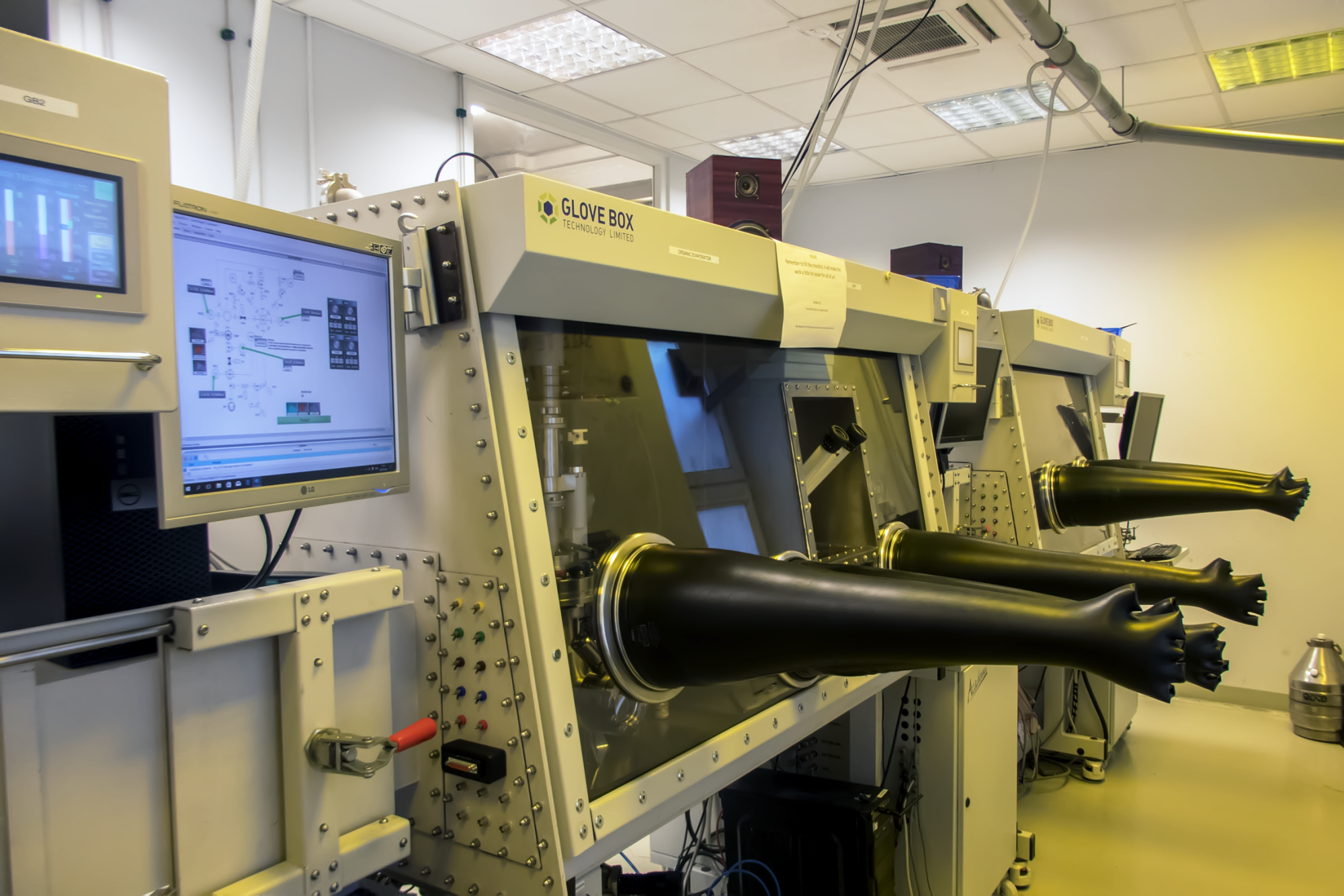
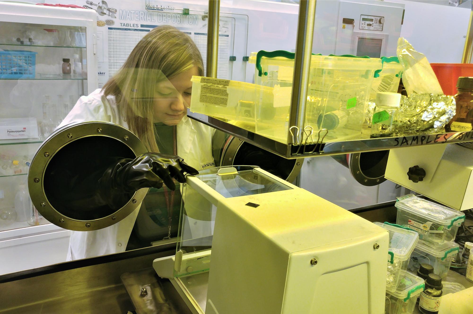
- Glove-Box system (5 chambers) with equipment
Parameters - equipment includes:
- System for thin layers fabrication Zone Casting technique
- System for thin layers fabrication Spin Coating technique
- Vacuum evaporation system for inorganic
- Inorganic and Organic materials evaporator system
- System for field-effect transistors measurements
- System for photovoltaic effect measurement (with sunlight simulator, AM1,5g)
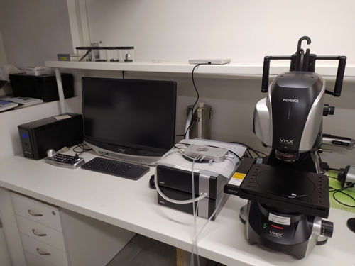
- High resolution digital microscope 4K Keyence serii VHX-S7000
Parameters:
The microscope consists of a motorized XYZ table, model VHX-S770E, and a set of lenses that allow the image to be magnified up to 2500x. The microscope is equipped with a number of improvements that allow the observation of samples at full depth of field, from various angles, as well as the option of constructing 3D profiles of the sample and assessing roughness. High Dynamic Range (HDR) imaging enables high color gradation. Observation of samples can be carried out in a Linkam temperature chamber operating in a wide temperature range.
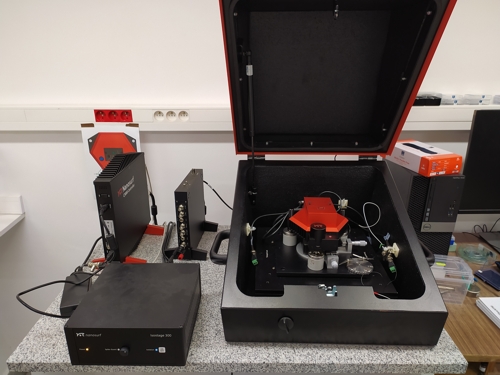
- Atomic Force Microscope Nanosurf FLexAFM
Parameters:
The microscope has a low-noise, high-resolution FlexAFM head with a scanning range of 10 x 10 x 3 micrometers and the ability to combine subsequent scanning areas to increase the analyzed area. The microscope is equipped with a C3000 digital controller that allows to achieve full 24-bit control precision of scanning and acquisition, and autonomous software that includes standard data acquisition modules and basic analysis options. The measurement can be performed in standard imaging modes: Static Force Mode, Lateral Force Mode, Dynamic Force Mode (Tapping Mode), Phase Imaging Mode, as well as in modes dependent on electric interactions: Electrostatic Force Microscopy (EFM) i Kelvin Probe Force Microscopy (KPFM).
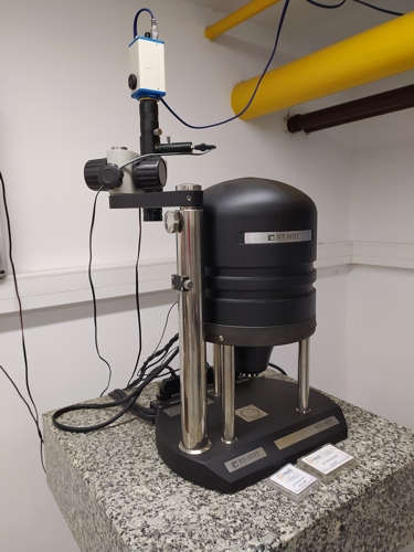
- Atomic Force Microscope AFM SolverPro NT-MDT
Parameters:
The microscope is equipped with heads with a scanning range of 120 x 120 x 3 micrometers. Measurements can be performed in standard imaging modes: Static Force Mode, Lateral Force Mode, Dynamic Force Mode (Tapping Mode), Phase Imaging Mode.
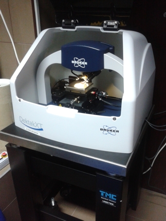
- Stylus Profiler (DektakXT-E, Bruker)
Parameters:
Measurement technique: contact measurement, step height repeatability: <5A, 1sigma on 0.1μm step, sensor type: thermally stable sensor LVDT with vertical resolution 1A max, base: high-polish glass (lambda /10) with base stability <1000A on 50mm range, optics: 3.1Mpx camera, color, installed under 45 degrees with on-line preview (digital zoom 1-4mm FOV), tip dimension: from 50nm (HAR tips available) to 25um, scan Length Range: 55mm max, vertical resolution: 1A max. (at 6.55um range), vertical range: 1mm max, sample height: 50mm max, stylus force: 1 to 15mg (Low Force Option from 0.03mg optional), sample X/Y stage: manual 100mm x 100mm, analytical functions: S, V, P parameters, step height, surface area, slope, volume analysis, data filters: Fourier, Histogram, statistical filters and Gauss filter.
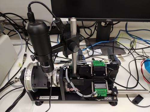
- A system of micromanipulators for testing the electrical parameters of transistors and a device for testing the electrical parameters of flexible transistors subjected to controlled deformation
- Unique, specially designed apparatus for:
- Automatic determination of photogeneration quantum yield using xerographic discharge system
- Simultaneous thermoluminescence and thermally stimulated current measurements
- Charge carrier recombination measurements with use of thermoluminescence technique
Contact person: Jaroslaw Jung, Adam Luczak, Izabela Bobowska
